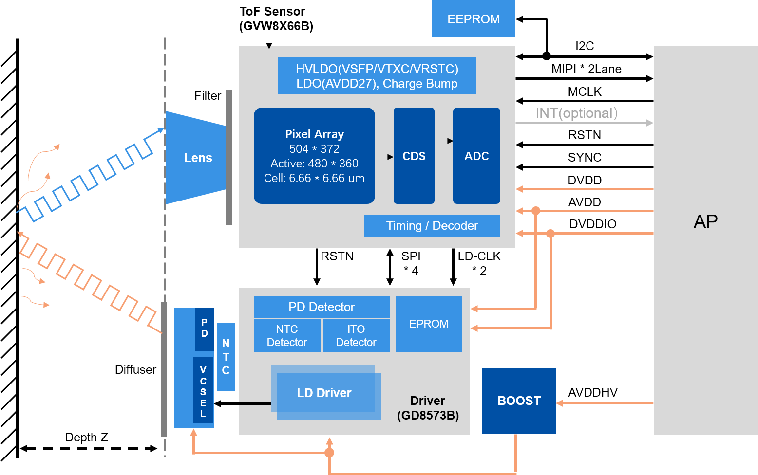
The GVW8366B is a ToF image sensor chip that can achieve HVGA (480*360) resolution through a backside illumination process to provide accurate depth information for smart devices. GVW8366B features a patented pixel architecture and an innovative working mode that combines the advantages of traditional CW-ToF and Pulse-ToF to achieve better ambient light suppression and lower power consumption. The proprietary programmable capability of receive pulse number enables single frame image with HDR (High Dynamic Range).The firmware architecture of pseudo random pulse train can greatly reduce the interference of multi devices.
Image performance
Resolution: 480 * 360(HVGA)
Pixel size: 6.6 μm * 6.6 μm
Interface: MIPI CSI-2
Transmission rate (Maximum): 750 Mbps * 2
QE: 33%@940 nm (Typical)
Support operation high light conditions: high light suppression
Demodulation frequency: 100 MHz (Maximum)
Support Hybrid-Mode (recommendation) and Pulse-Mode demodulation
Pulse width (Minimum): 5 ns
Peripheral control interface
CCI, support 1 Mbps
SPI
Ambient light suppression (maximum): 100 Klux

Open WeChat, use "Scan" to follow.
