
The Goodix GR533x series is a comprehensive-performance Bluetooth LE 5.3 SoC designed for various applications such as smart home, health care, smart trackers, and IoT modules, supporting Bluetooth Mesh networking protocols.
Based on Arm® Cortex®-M4F CPU core running at 64 MHz, the GR533x integrates a 2.4 GHz RF transceiver, Bluetooth LE 5.3 protocol stack, 512 KB on-chip Flash memory, 96 KB system SRAM, and a rich set of peripherals. It provides outstanding RF performance, featuring a maximum TX power of +15 dBm, an RX sensitivity of -99 dBm in Bluetooth LE 1 Mbps mode, achieving a total link budget of up to 114 dB.
With two main power supply schemes (DC-DC and SYS_LDO), the GR533x offers flexible options to achieve a balance between low power consumption and economical BOM.
Bluetooth Low Energy 5.3 transceiver integrating Controller and Host layers
Supported data rates: 1 Mbps, 2 Mbps, Long Range (500 kbps, 125 kbps)
TX power:
GR5330/GR5331: up to 6 dBm
GR5332: up to 15 dBm
RX sensitivity:
GR5330/GR5331: -97.5 dBm @ 1 Mbps
GR5332: -99 dBm @ 1 Mbps
Power consumption at 3.3 V VBAT input on GR5330/GR5331:
TX current: 3.8 mA @ 0 dBm output power (DC-DC supply, 16 MHz system clock)
RX current: 4.7 mA @ 1 Mbps (DC-DC supply, 16 MHz system clock)
Power consumption at 3.3 V VBAT input on GR5332:
TX current: 5.9 mA @ 0 dBm output power (DC-DC supply, 16 MHz system clock)
TX current: 86.3 mA @ 15 dBm output power (SYS_LDO supply, 64 MHz system clock)
RX current: 4.9 mA @ 1 Mbps (DC-DC supply, 16 MHz system clock)
Arm® Cortex®-M4F 32-bit micro-processor with floating point support
Up to 64 MHz clock frequency
Built-in Memory Protection Unit (MPU) supporting eight programmable regions
Hardware Floating Point Unit (FPU)
Built-in Nested Vectored Interrupt Controller (NVIC)
Non-maskable Interrupt (NMI) input
Serial Wire Debug (SWD) with 16 breakpoints, two watchpoints, and a debug timestamp counter
32 µA/MHz CoreMark running from Flash @ 3.3 V, 64 MHz
On-chip memory
ROM for chip bootloader, system drivers, and Bluetooth LE Protocol Stack code
RAM for data and instruction code, with retention capabilities in sleep mode(GR5331/GR5332: 96 KB,GR5330: 64 KB )
512 KB Flash for code, system parameter configuration, and user data
Digital peripheral
One general-purpose DMA engine with five channels and up to 16 programmable request/trigger sources
Analog peripherals
One 13-bit Sense ADC with a sampling rate of 1 Msps. It supports up to eight external I/O channels and three internal signal channels
Built-in die temperature and voltage sensors
Low-power comparator, supporting wakeup from sleep mode
Flexible serial peripherals
Two UART modules up to 2 Mbps with flow control and IrDA features
Two I2C modules for peripheral communication, up to 1 MHz
One 8-bit/16-bit/32-bit SPI master interface and one SPI slave interface for host communication
Security
Complete secure computing engine
AES 128-bit security module (ECB, CBC)
True random number generator (TRNG)
I/O peripherals
Up to 32 multiplexed I/O pins in total
Up to 14 general-purpose I/O (GPIO) pins with configurable pull-up/pull-down resistors
Up to eight always-on I/O (AON I/O) pins, supporting wakeup from sleep mode
Up to 10 mixed signal I/O (MSIO) pins, configurable to be digital/analog signal interfaces
Timers
Two general-purpose, 32-bit timer modules
One dual timer module composed of two programmable 32-bit or 16-bit down counters
One sleep timer for waking the device up from sleep mode
Two 3-channel PWM modules with edge alignment mode and center alignment mode
One real-time counter (RTC)
Power management
On-chip DC-DC/SYS_LDO to provide RF analog voltage and supply CORE_LDO
On-chip I/O LDO to provide I/O voltage and supply external components
Programmable thresholds for brownout detector (BOD)
Supply voltage: 2.0 V – 3.63 V
I/O voltage: 1.8 V – 3.6 V
Low-power consumption
Sleep mode: 2.6 µA (Typical) at 3.3 V VBAT input, with 48 KB SRAM retention on, wakeup sources from AON I/Os, and LFXO_32K running
Ultra deep sleep mode: 2.2 µA (Typical), with no memory data in retention and wakeup sources from SLP Timer or AON I/Os
OFF mode: 200 nA (Typical), with system in reset mode
Packages
QFN32: 4.0 mm * 4.0 mm * 0.75 mm, 0.4 mm pitch
QFN48: 6.0 mm * 6.0 mm * 0.75 mm, 0.4 mm pitch
BGA45: 3.0 mm * 3.0 mm * 0.67 mm, 0.4/0.5 mm pitch
Operating temperature range
GR5330/GR5331: –40°C ~ 85°C
GR5332: –40°C ~ 105°C
|
GR5330AENI | GR5331AENI |
GR5331CENI |
GR5331DEBI |
GR5332AENE |
GR5332CENE |
|
|---|---|---|---|---|---|---|---|
Status |
Active |
Active |
Active |
Active |
Active |
Active |
|
Protocol |
Bluetooth LE[1] |
5.3 |
5.3 |
5.3 |
5.3 |
5.3 |
5.3 |
Bluetooth Mesh |
● |
● |
● |
● |
● |
● |
|
Core System |
CPU |
Cortex®-M4F |
Cortex®-M4F |
Cortex®-M4F |
Cortex®-M4F |
Cortex®-M4F |
Cortex®-M4F |
Clocks |
64 MHz / 32 kHz |
64 MHz / 32 kHz |
64 MHz / 32 kHz |
64 MHz / 32 kHz |
64 MHz / 32 kHz |
64 MHz / 32 kHz |
|
Cache |
8 KB |
8 KB |
8 KB |
8 KB |
8 KB |
8 KB |
|
RAM |
64 KB |
96 KB |
96 KB |
96 KB |
96 KB |
96 KB |
|
OTP |
● |
● |
● |
● |
● |
● |
|
Flash |
512 KB |
512 KB |
512 KB |
512 KB |
512 KB |
512 KB |
|
Security |
AES-128 |
● |
● |
● |
● |
● |
● |
TRNG |
● |
● |
● |
● |
● |
● |
|
Radio |
Frequency |
2.4 GHz |
2.4 GHz |
2.4 GHz |
2.4 GHz |
2.4 GHz |
2.4 GHz |
Maximum TX Power |
6 dBm |
6 dBm |
6 dBm |
2.4 GHz |
15 dBm |
15 dBm |
|
RX Sensitivity |
-97.5 dBm (@ 1 Mbps) |
-97.5 dBm (@ 1 Mbps) |
-97.5 dBm (@ 1 Mbps) |
-97.5 dBm (@ 1 Mbps) |
-99 dBm (@ 1 Mbps) |
-99 dBm (@ 1 Mbps) |
|
Peripheral |
UART |
2 |
2 |
2 |
2 |
2 |
2 |
SPI |
1 * SPIM / 1 * SPIS |
1 * SPIM / 1 * SPIS |
1 * SPIM / 1 * SPIS |
1 * SPIM / 1 * SPIS |
1 * SPIM / 1 * SPIS |
1 * SPIM / 1 * SPIS |
|
I2C |
2 | 2 |
2 |
2 |
2 |
2 |
|
Timers |
4 | 4 |
4 |
4 |
4 |
4 |
|
PWM |
2 | 2 |
2 |
2 |
2 |
2 |
|
RTC |
1 | 1 |
1 |
1 |
1 |
1 |
|
ADC |
13-bit |
13-bit |
13-bit |
13-bit |
13-bit |
13-bit |
|
Comparator |
● |
● |
● |
● |
● |
● |
|
Temperature Sensor |
● |
● |
● |
● |
● |
● |
|
GPIO |
16 |
16 |
32 |
31 |
16 |
32 |
|
Packages |
Type |
QFN32 |
QFN32 |
QFN48 |
BGA45 |
QFN32 |
QFN48 |
Dimensions |
4.0 mm * 4.0 mm |
4.0 mm * 4.0 mm |
6.0 mm * 6.0 mm |
3.0 mm * 3.0 mm |
4.0 mm * 4.0 mm |
6.0 mm * 6.0 mm |
|
Certification |
SIG BQB (QDID: 179976) | ||||||
Operating Temperature |
-40℃ - 85℃ |
-40℃ - 85℃ |
-40℃ - 85℃ |
-40℃ - 85℃ |
-40℃ - 105℃ |
-40℃ - 105℃ |
|
Supply Voltage Range |
2.0 V - 3.63 V |
2.0 V - 3.63 V |
2.0 V - 3.63 V |
2.0 V - 3.63 V |
2.0 V - 3.63 V |
2.0 V - 3.63 V |
|
Development Kits |
GR5331 Starter Kit |
GR5331 Starter Kit |
GR5331 Starter Kit |
|
GR5331 Starter Kit |
GR5331 Starter Kit |
|
Notes: |
|||||||
|
GR5330AENI | GR5331AENI |
GR5331CENI |
GR5331DEBI |
GR5332AENE |
GR5332CENE |
|
|---|---|---|---|---|---|---|---|
Status |
Active |
Active |
Active |
Active |
Active |
Active |
|
Protocol |
Bluetooth LE[1] |
5.3 |
5.3 |
5.3 |
5.3 |
5.3 |
5.3 |
Bluetooth Mesh |
● |
● |
● |
● |
● |
● |
|
Core System |
CPU |
Cortex®-M4F |
Cortex®-M4F |
Cortex®-M4F |
Cortex®-M4F |
Cortex®-M4F |
Cortex®-M4F |
Clocks |
64 MHz / 32 kHz |
64 MHz / 32 kHz |
64 MHz / 32 kHz |
64 MHz / 32 kHz |
64 MHz / 32 kHz |
64 MHz / 32 kHz |
|
Cache |
8 KB |
8 KB |
8 KB |
8 KB |
8 KB |
8 KB |
|
RAM |
64 KB |
96 KB |
96 KB |
96 KB |
96 KB |
96 KB |
|
OTP |
● |
● |
● |
● |
● |
● |
|
Flash |
512 KB |
512 KB |
512 KB |
512 KB |
512 KB |
512 KB |
|
Security |
AES-128 |
● |
● |
● |
● |
● |
● |
TRNG |
● |
● |
● |
● |
● |
● |
|
Radio |
Frequency |
2.4 GHz |
2.4 GHz |
2.4 GHz |
2.4 GHz |
2.4 GHz |
2.4 GHz |
Maximum TX Power |
6 dBm |
6 dBm |
6 dBm |
2.4 GHz |
15 dBm |
15 dBm |
|
RX Sensitivity |
-97.5 dBm (@ 1 Mbps) |
-97.5 dBm (@ 1 Mbps) |
-97.5 dBm (@ 1 Mbps) |
-97.5 dBm (@ 1 Mbps) |
-99 dBm (@ 1 Mbps) |
-99 dBm (@ 1 Mbps) |
|
Peripheral |
UART |
2 |
2 |
2 |
2 |
2 |
2 |
SPI |
1 * SPIM / 1 * SPIS |
1 * SPIM / 1 * SPIS |
1 * SPIM / 1 * SPIS |
1 * SPIM / 1 * SPIS |
1 * SPIM / 1 * SPIS |
1 * SPIM / 1 * SPIS |
|
I2C |
2 | 2 |
2 |
2 |
2 |
2 |
|
Timers |
4 | 4 |
4 |
4 |
4 |
4 |
|
PWM |
2 | 2 |
2 |
2 |
2 |
2 |
|
RTC |
1 | 1 |
1 |
1 |
1 |
1 |
|
ADC |
13-bit |
13-bit |
13-bit |
13-bit |
13-bit |
13-bit |
|
Comparator |
● |
● |
● |
● |
● |
● |
|
Temperature Sensor |
● |
● |
● |
● |
● |
● |
|
GPIO |
16 |
16 |
32 |
31 |
16 |
32 |
|
Packages |
Type |
QFN32 |
QFN32 |
QFN48 |
BGA45 |
QFN32 |
QFN48 |
Dimensions |
4.0 mm * 4.0 mm |
4.0 mm * 4.0 mm |
6.0 mm * 6.0 mm |
3.0 mm * 3.0 mm |
4.0 mm * 4.0 mm |
6.0 mm * 6.0 mm |
|
Certification |
SIG BQB (QDID: 179976) | ||||||
Operating Temperature |
-40℃ - 85℃ |
-40℃ - 85℃ |
-40℃ - 85℃ |
-40℃ - 85℃ |
-40℃ - 105℃ |
-40℃ - 105℃ |
|
Supply Voltage Range |
2.0 V - 3.63 V |
2.0 V - 3.63 V |
2.0 V - 3.63 V |
2.0 V - 3.63 V |
2.0 V - 3.63 V |
2.0 V - 3.63 V |
|
Development Kits |
GR5331 Starter Kit |
GR5331 Starter Kit |
GR5331 Starter Kit |
GR5331 Starter Kit |
GR5331 Starter Kit |
GR5331 Starter Kit |
|
Notes: |
|||||||
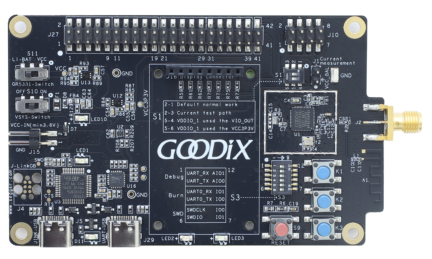
GR5331 Starter Kit
GR5331 Starter Kit (GR5331 SK) is a Goodix proprietary platform that helps users quickly get started with project evaluation, development, debugging, and performance verification for GR533x series SoCs.
Read More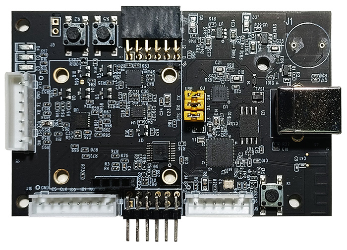


Added GR5331DEBI reference design files.
Updated pin mux table.
Added GR5330AENI reference design files
Updated the value of C4 in the matching circuit of GR5331 reference designs
Updated the recommended FB1 material
Including the reference schematic designs for the minimal system operation, recommended BOM, and Pin Mux tables of GR533x SoCs
Updated the schematics and BOMs for the module reference designs
Including the module reference design for the GR533x SoCs in QFN32 package to help users in designing compact module projects
| Name | Rights Description | Version | Date |
|---|---|---|---|
| GR533x Product Brief | For Public | Rev.1.4 | 2025-04-27 |
| GR533x Datasheet | For Public | Rev.1.5 | 2025-04-25 |
| GR5xx IAR User Manual | For Public | Rev.1.2 | 2025-08-06 |
| GR5xx GCC User Manual | For Public | Rev.1.2 | 2025-08-06 |
| GR5331 Starter Kit User Guide | For Public | Rev.1.2 | 2025-04-27 |
| GR5xx Mesh Demo User Manual | For Public | Rev.1.0 | 2025-04-25 |
| GProgrammer User Manual | For Public | Rev.3.3 | 2025-04-25 |
| GRPLT User Manual | For Public | Rev.2.9 | 2025-04-25 |
| GR533x Developer Guide | For Public | Rev.1.4 | 2025-04-25 |
| GRPLT Lite Config Tool User Manual | For Public | Rev.1.7 | 2024-06-18 |
| PLT Lite User Manual | For Public | Rev.1.0 | 2023-11-28 |
GR5331 Starter Kit
A development kit based on GR533x SoC which is designed for quick learning about GR533x development environment.
Read More
Open WeChat, use "Scan" to follow.

