
The Goodix GR5525 series is a comprehensive-performance single-mode Bluetooth LE 5.3 SoC designed to deliver outstanding performance. Built upon various technology advantages and new features, it can be flexibly configured as a Broadcaster, an Observer, a Peripheral, or a Central. Moreover, it supports the flexible combination of all the above roles, making it an ideal choice for Internet of Things (IoT) and smart wearable devices.
Based on ARM® Cortex® -M4F CPU core, the GR5525 series integrates Bluetooth 5.3 Protocol Stack, a 2.4 GHz RF transceiver, on-chip programmable Flash memory, RAM, and multiple peripherals. It provides up to four I2C/UART interfaces, expands the I/O functionality, and enhances the QSPI interface, covering a wider range of IoT and wearable applications.
Bluetooth Low Energy 5.3 transceiver integrating Controller and Host layers
Supported data rates: 1 Mbps, 2 Mbps, Long Range (500 kbps, 125 kbps)
TX power: -20 dBm to +7 dBm
-97 dBm sensitivity (in 1 Mbps mode)
-93 dBm sensitivity (in 2 Mbps mode)
-101 dBm sensitivity (in Long Range 500 kbps mode)
-103 dBm sensitivity (in Long Range 125 kbps mode)
TX current: 6.3 mA @ 0 dBm, 1 Mbps, 64 MHz
RX current: 5.3 mA @ 1 Mbps, 64 MHz
ARM®Cortex®-M4F 32-bit micro-processor with floating point support
Up to 96 MHz clock frequency
Built-in Memory Protection Unit (MPU) supporting eight programmable regions
Hardware Floating Point Unit (FPU)
Built-in Nested Vectored Interrupt Controller (NVIC)
Non-maskable Interrupt (NMI) input
Serial Wire Debug (SWD) with 16 breakpoints, two watchpoints, and a debug timestamp counter
56 µA/MHz CoreMark running from Flash @ 3.3 V, 64 MHz
On-chip memory
ROM for chip bootloader, system drivers, and Bluetooth LE Protocol Stack code
256 KB RAM for data and instruction code, with retention capabilities in sleep mode
Flash for code, system parameter configuration, and user data (GR5525I0NI: external Flash,GR5525IENI: 512KB,GR5525RGNI: 1MB)
Digital peripherals
Two general-purpose DMA engines, each with six channels and up to 16 programmable request/trigger sources
Analog peripherals
One 13-bit Sense ADC with a sampling rate of 1 Msps. It supports up to eight external I/O channels and three internal signal channels
Built-in die temperature and voltage sensors
Low-power comparator, supporting wakeup from sleep mode
Flexible serial peripherals
Four UART modules up to 2 Mbps with all modules supporting flow control and IrDA
Four I2C modules for peripheral communication, up to 3.4 MHz
One 8-bit/16-bit/32-bit SPI master interface and one SPI slave interface for host communication
Two I2S interfaces (one I2S master interface and one I2S slave interface)
PDM interface with hardware sampling rate converter
One Dual-lane SPI (DSPI) interface for display, with MIPI DBI Type-C support
Three Quad SPI (QSPI) interfaces, up to 48 MHz; supporting direct access via memory mapping when connecting with external NOR Flash
Security
Complete secure computing engine:
AES 128-bit/192-bit/256-bit symmetric encryption (ECB, CBC)
Hash-based Message Authentication Code (HMAC-SHA256)
PKC
TRNG
Comprehensive security operation mechanism:
Secure boot
Encrypted firmware runs directly from Flash
eFuse for encrypted key storage
Differentiate application data key and firmware key, supporting one data per device/product
I/O peripherals
Up to 50 multiplexed I/O pins in total
Up to 34 general-purpose I/O (GPIO) pins
Up to eight always-on I/O (AON IO) pins, supporting wakeup from sleep mode
Up to eight mixed signal I/O (MSIO) pins, configurable to be digital/analog signal interfaces
Timer
Two general-purpose, 32-bit timer modules
A dual timer module composed of two programmable 32-bit or 16-bit down counters
An internal sleep timer that can be used to wake the device up from sleep mode
Two PWM modules with edge alignment mode and center alignment mode, each with three channels
Two real-time counters (RTC): one RTC and one Calendar
Power management
On-chip DC-DC to provide RF analog voltage and supply core LDO
On-chip I/O LDO to provide I/O voltage and supply external components; maximum I/O LDO drive strength: 30 mA
Programmable thresholds for brownout detection (BOD)
Supply voltage: 2.4 V – 3.8 V
I/O voltage: 1.8 V – 3.6 V
Low-power consumption
Sleep mode: 7.3 µA (Typical) at 3.3 V VBAT input with SRAM retention on and LFXO_32K running; woken up by eight sources of always-on domain
Ultra deep sleep mode: 5.0 µA (Typical); internal power (all SRAM included) and LFXO_32K removed from entire chip except always-on domain; woken up by Sleep Timer and AON GPIOs
OFF mode: 200 nA (Typical); nothing on except VBAT, and chip in reset mode
Packages
QFN68: 7.0 mm * 7.0 mm * 0.85 mm, 0.35 mm pitch
QFN56: 7.0 mm * 7.0 mm * 0.75 mm, 0.4 mm pitch
Operating temperature range: -40 °C to +85 °C
|
GR5525RGNI |
GR5525IENI |
GR5525I0NI |
|
|---|---|---|---|---|
Status |
Active |
Active |
Active |
|
Protocol |
Bluetooth LE [1] |
5.3 |
5.3 |
5.3 |
Bluetooth Mesh |
● |
● |
● |
|
Core System |
CPU |
Cortex®-M4F |
Cortex®-M4F |
Cortex®-M4F |
Clocks |
96 MHz / 32kHz |
96 MHz / 32kHz |
96 MHz / 32kHz |
|
Cache |
8 KB |
8 KB |
8 KB |
|
RAM |
256 KB |
256 KB |
256 KB |
|
OTP |
|
|
|
|
Flash |
1 MB |
512 KB |
External Flash |
|
Security |
Root of Trust |
● |
● |
● |
Secure Key Store |
4 |
4 |
4 |
|
PKC |
● |
● |
● |
|
RSA |
● |
● |
● |
|
AES |
● |
● |
● |
|
ECC |
● |
● |
● |
|
TRNG |
● |
● |
● |
|
Radio |
Frequency |
2.4 GHz |
2.4 GHz |
2.4 GHz |
Maximum TX Power |
7 dBm |
7 dBm |
7 dBm |
|
RX Sensitivity |
-97 dBm (@1Mbps) |
-97 dBm (@1Mbps) |
-97 dBm (@1Mbps) |
|
Peripheral |
UART |
4 |
4 |
4 |
SPI |
1 * SPIM / 1 * SPIS |
1 * SPIM / 1 * SPIS |
1 * SPIM / 1 * SPIS |
|
I2C |
4 |
4 |
4 |
|
QSPI |
3 |
3 |
3 |
|
DSPI |
1 |
1 |
1 |
|
Timers |
4 |
4 |
4 |
|
PWM |
2 |
2 |
2 |
|
RTC |
2 |
2 |
2 |
|
I2S |
1 * I2SM / 1 * I2SS |
1 * I2SM / 1 * I2SS |
1 * I2SM / 1 * I2SS |
|
PDM |
● |
● |
● |
|
ADC |
13-bit |
13-bit |
13-bit |
|
Comparator |
● |
● |
● |
|
Temperature Sensor |
● |
● |
● |
|
GPIO |
50 |
39 |
39 |
|
Packages |
Type |
QFN68 |
QFN56 |
QFN56 |
Dimensions |
7.0 * 7.0 mm |
7.0 * 7.0 mm |
7.0 * 7.0 mm |
|
Certification |
SIG BQB (QDID: 179976) |
|||
Operating Temperature |
-40℃ - 85℃ |
-40℃ - 85℃ |
-40℃ - 85℃ |
|
Supply Voltage Range |
2.4 V - 3.8 V |
2.4 V - 3.8 V |
2.4 V - 3.8 V |
|
Development Kits |
GR5525 Starter Kit |
GR5525 Starter Kit |
GR5525 Starter Kit |
|
Notes: |
||||
|
GR5525RGNI |
GR5525IENI |
GR5525I0NI |
|
|---|---|---|---|---|
Status |
Active |
Active |
Active |
|
Protocol |
Bluetooth LE [1] |
5.3 |
5.3 |
5.3 |
Bluetooth Mesh |
● |
● |
● |
|
Core System |
CPU |
Cortex®-M4F |
Cortex®-M4F |
Cortex®-M4F |
Clocks |
96 MHz / 32kHz |
96 MHz / 32kHz |
96 MHz / 32kHz |
|
Cache |
8 KB |
8 KB |
8 KB |
|
RAM |
256 KB |
256 KB |
256 KB |
|
OTP |
|
|
|
|
Flash |
1 MB |
512 KB |
External Flash |
|
Security |
Root of Trust |
● |
● |
● |
Secure Key Store |
4 |
4 |
4 |
|
PKC |
● |
● |
● |
|
RSA |
● |
● |
● |
|
AES |
● |
● |
● |
|
ECC |
● |
● |
● |
|
TRNG |
● |
● |
● |
|
Radio |
Frequency |
2.4 GHz |
2.4 GHz |
2.4 GHz |
Maximum TX Power |
7 dBm |
7 dBm |
7 dBm |
|
RX Sensitivity |
-97 dBm (@1Mbps) |
-97 dBm (@1Mbps) |
-97 dBm (@1Mbps) |
|
Peripheral |
UART |
4 |
4 |
4 |
SPI |
1 * SPIM / 1 * SPIS |
1 * SPIM / 1 * SPIS |
1 * SPIM / 1 * SPIS |
|
I2C |
4 |
4 |
4 |
|
QSPI |
3 |
3 |
3 |
|
DSPI |
1 |
1 |
1 |
|
Timers |
4 |
4 |
4 |
|
PWM |
2 |
2 |
2 |
|
RTC |
2 |
2 |
2 |
|
I2S |
1 * I2SM / 1 * I2SS |
1 * I2SM / 1 * I2SS |
1 * I2SM / 1 * I2SS |
|
PDM |
● |
● |
● |
|
ADC |
13-bit |
13-bit |
13-bit |
|
Comparator |
● |
● |
● |
|
Temperature Sensor |
● |
● |
● |
|
GPIO |
50 |
39 |
39 |
|
Packages |
Type |
QFN68 |
QFN56 |
QFN56 |
Dimensions |
7.0 * 7.0 mm |
7.0 * 7.0 mm |
7.0 * 7.0 mm |
|
Certification |
SIG BQB (QDID: 179976) |
|||
Operating Temperature |
-40℃ - 85℃ |
-40℃ - 85℃ |
-40℃ - 85℃ |
|
Supply Voltage Range |
2.4 V - 3.8 V |
2.4 V - 3.8 V |
2.4 V - 3.8 V |
|
Development Kits |
GR5525 Starter Kit |
GR5525 Starter Kit |
GR5525 Starter Kit |
|
Notes: |
||||
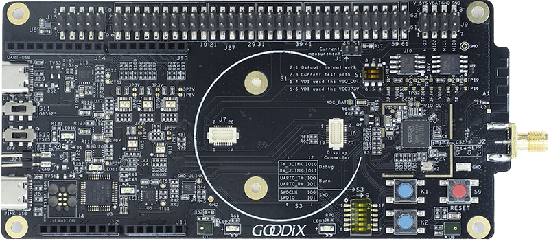
GR5525 Starter Kit
GR5525 Starter Kit (GR5525 SK) is a Goodix proprietary platform that helps users quickly get started with project evaluation, development, debugging, and performance verification for GR5525 series SoCs.
Read More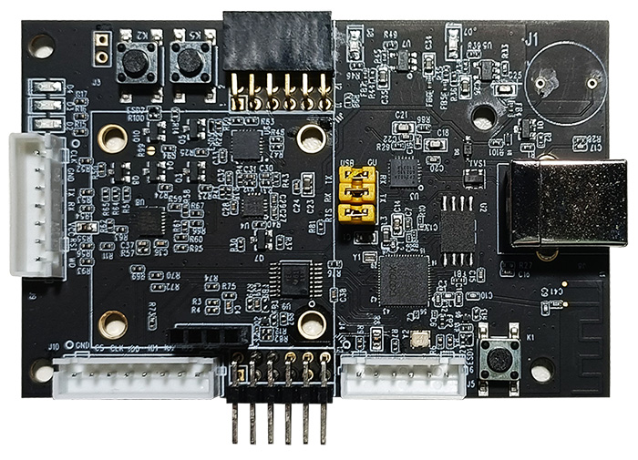


Deleted GR5525IGNI reference design files.
Added a 2.2 μF capacitor to the RC circuit at the VBATL pin.
Including the reference schematic designs for the minimal system operation, recommended BOM, and Pin Mux tables of GR5525 SoCs
| Name | Rights Description | Version | Date |
|---|---|---|---|
| GR5525 Product Brief | For Public | Rev.1.1 | 2024-09-23 |
| GR5525 Datasheet | For Public | Rev.1.4 | 2025-08-06 |
| GR5525 Developer Guide | For Public | Rev.1.3 | 2025-08-06 |
| GR5xx IAR User Manual | For Public | Rev.1.2 | 2025-08-06 |
| GR5xx GCC User Manual | For Public | Rev.1.2 | 2025-08-06 |
| GR5525 Starter Kit User Guide | For Public | Rev.1.3 | 2025-04-27 |
| GProgrammer User Manual | For Public | Rev.3.3 | 2025-04-25 |
| GRPLT User Manual | For Public | Rev.2.9 | 2025-04-25 |
| GR5525 Display Refresh Module Guide | For Public | Rev.1.2 | 2024-09-23 |
| GRPLT Lite Config Tool User Manual | For Public | Rev.1.7 | 2024-06-18 |
| GR5525 Reference Design | Register Users Only | Rev.1.3 | 2024-09-23 |

GR5525 Starter Kit
A development kit based on GR5525 SoC which is designed for quick learning about GR5525 development environment.
View More
Open WeChat, use "Scan" to follow.

